Understanding the Role of Semiconductor Processing Equipment
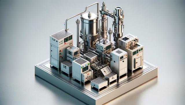
Semiconductor Processing Equipment: Solutions for Precision Manufacturing encompasses a wide range of tools and systems that are essential for producing integrated circuits with extreme accuracy. These tools are used in various stages of semiconductor fabrication, including deposition, lithography, etching, cleaning, and inspection. The complexity and miniaturization of modern chips demand equipment that can operate at microscopic scales with minimal tolerances. As such, manufacturers rely heavily on precision-engineered machinery to ensure consistency and quality across every wafer.
Each phase of the manufacturing process requires specific equipment designed to perform highly controlled tasks. For example, photolithography systems project patterns onto silicon wafers, while etching machines remove unwanted material with nanometer-scale accuracy. The advancement of such tools directly impacts the capability to produce faster, smaller, and more energy-efficient semiconductor devices.
Key aspects that define effective semiconductor processing equipment include:
- High-resolution patterning capabilities
- Contamination control and cleanroom compatibility
- Repeatable and stable operation over long production runs
- Integration with monitoring systems for quality assurance
Overall, these systems enable the transformation of raw silicon into functional and high-performing microchips.
Precision in Lithography and Etching Processes
Among the most critical steps in semiconductor fabrication are lithography and etching, both of which rely on exceptional precision. Lithography tools use ultraviolet light to transfer circuit designs onto photoresist-coated wafers. The accuracy of this process determines the minimum feature size achievable on a chip. As device geometries continue to shrink, the demand for advanced lithography systems—such as those using extreme ultraviolet (EUV) light—has increased significantly.
Etching follows lithography and involves selectively removing layers of material to create the desired patterns. Dry etching systems, like reactive ion etching (RIE), offer fine control over depth and uniformity, which is essential for multi-layered chip designs. These processes must operate within ultra-clean environments to avoid defects caused by particulate contamination.
Several challenges addressed by modern lithography and etching equipment include:
- Maintaining alignment accuracy across wafers
- Achieving high aspect ratio features without collapse
- Minimizing line edge roughness for signal integrity
Solutions for Precision Manufacturing in this area involve continuous innovation in optics, plasma technologies, and automation systems to meet evolving design rules.
Deposition and Cleaning Equipment for Material Integrity
Deposition processes lay the foundation for semiconductor structures by adding thin films of material onto wafers. Techniques such as physical vapor deposition (PVD), chemical vapor deposition (CVD), and atomic layer deposition (ALD) are commonly used. These methods must ensure uniform coverage, precise thickness control, and excellent adhesion properties.
Cleaning equipment plays a vital role in maintaining the purity of wafer surfaces before and after each process step. Even microscopic particles can lead to defects in the final chip, making high-efficiency cleaning tools indispensable. Wet benches, megasonic cleaners, and advanced scrubbers are among the systems used to eliminate contaminants without damaging delicate structures.
Modern deposition and cleaning tools are engineered with the following capabilities:
- In-situ monitoring for film thickness and uniformity
- Automated material handling to reduce human contact
- Compatibility with advanced materials like high-k dielectrics and metal gates
By ensuring both the structural and chemical integrity of each layer, these solutions support reliable and scalable semiconductor manufacturing.
Advanced Inspection and Metrology Systems
Inspection and metrology equipment provide critical feedback throughout the semiconductor fabrication process. These systems allow manufacturers to detect defects, measure feature dimensions, and verify layer alignment with sub-nanometer accuracy. As chips become more complex, the role of inspection tools grows increasingly important to maintain yield and performance standards.
Optical and electron beam inspection systems can identify surface and sub-surface anomalies, while metrology tools measure parameters such as film thickness, critical dimensions, and overlay accuracy. Automated defect classification and data analytics further enhance production efficiency by enabling predictive maintenance and real-time process adjustments.
Notable functions of modern inspection and metrology equipment include:
- High-speed scanning of entire wafers
- Non-destructive testing methods
- Data integration with process control systems
These capabilities contribute to cost-effective manufacturing by reducing scrap rates and enabling faster time-to-market for new technologies. As part of the broader category of Semiconductor Processing Equipment: Solutions for Precision Manufacturing, these tools play a central role in ensuring product consistency and reliability.
Automation and Integration for Scalable Production
Scalability and throughput are essential in semiconductor manufacturing, and automation greatly contributes to achieving these goals. Fully automated systems can handle wafer transport, process execution, and quality control with minimal human intervention. This not only improves productivity but also reduces the risk of contamination and handling errors.
Equipment integration through factory automation software enables seamless communication between different tools and facilitates process optimization. This interconnected approach allows for real-time monitoring and adaptive control, helping to maintain consistent output even as production volumes increase.
Key automation features in semiconductor processing environments include:
- Robotic wafer handling systems
- Advanced scheduling and dispatch systems
- Integrated data collection and analytics platforms
By leveraging automation alongside precision tools, manufacturers can scale operations efficiently while maintaining the exacting standards required for modern chip production. Semiconductor Processing Equipment: Solutions for Precision Manufacturing continues to evolve with smart manufacturing trends, enabling more responsive and agile fabrication lines.
Conclusion: Supporting Innovation Through Precision Technology
For manufacturers in the semiconductor industry, investing in reliable and precise processing equipment is essential to meet the demands of advanced chip designs. From lithography and etching to cleaning and inspection, each process is tightly controlled by specialized tools that ensure accuracy, reproducibility, and cleanliness. By adopting Semiconductor Processing Equipment: Solutions for Precision Manufacturing, companies can enhance yield, reduce defects, and accelerate innovation. As the industry moves toward increasingly complex architectures, the role of precision manufacturing solutions becomes even more critical in delivering the next generation of electronic devices.


Leave a Reply